


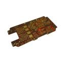
double sided pcb copper thickness
Product Description
How to make professional double-sided PCB with CNC milling machine?
Step 1: Parts and parts tools
How to make professional double-sided PCB with CNC milling machine
tool
CNC milling machine:
3.175 mm chuck (such as ER11 chuck)
Z probe
Nail gun (used to make vias)
Hammer (used to hit nails)
Sandpaper (fine mesh)
Ultraviolet rays
Cheap CNC is fully capable of this job. The Chinese unit is about US$150-300.
Components
PCB blank/copper clad board
PCB milling cutter: 0.2 mm, 30° tip
PCB drill bits: 1 mm and 1.5 mm
PCB milling cutter: 2 mm and 3 mm
PCB rivets: 0.9 mm and 1.3 mm outer diameter
PCB UV curing solder mask (green)
Correction fluid (tipp-ex)
3 mm positioning pin
PCB and aluminum alloy header
Liquid tin/chemical tin solution (optional)
All parts can be found on aliexpress or ebay, and the prices are as above. Chemical tin solutions can be more difficult to find and can be very expensive (around $50 for a bottle), but they are completely optional.
The PCB bracket and the positioning pin bracket are used to install the PCB on the CNC bed. You can print them from the zip file or the original designer, 2 copies are required for each file.
Step 2: Software
In addition to the CNC milling machine and some tools, we also need 3 programs to make our own PCB
PCB design software to design PCB
Flatcam to generate code for CNC milling machine
Candle control CNC milling cutter
PCB design software
You can use any PCB design software you want. Popular choices include: Altium designer, Circuitmaker, Eagle, Kicad,...I will assume that you know how to design a PCB and export Gerber files. If you don't know what these are, creating a gerber file for a PCB is like generating a PDF for a text file. It is a standard format for saving PCB specifications. You can find many tutorials online.
Flatcam
Flatcam is not very common, but very easy to use. I will explain each step in detail and guide you through the process. If in doubt, check out the excellent Flatcam manual.
Flatcam will take our gerber file and convert it into machine motion (gcode) through a technique called isolated routing. To mill a PCB track, we must mill the contour of the track to isolate it from the surrounding copper, hence the name.

Selected: Used to generate new files
Option: Used to store the default settings
Tool: for double-sided PCB
We first use File> Open Gerber to open a gerber file, which will be displayed under the project tab. Now there are 3 steps to convert this gerber to gcode:
Generate isolation tool path
Click the gerber file in the project tab to select it, and then click the selected tab
Here, we can enter the settings of the tool we will use and click Generate Geometry
Go back to the project tab and we are in the extension
Generate geometry
Click the item tab to select it and click the selected tab
Now we enter the cutting depth and speed, and click generate
Return to the project tab
Export gcode
Click the cnc file in the project tab to select it, then click the selected tab
Click Export gcode and save the file with the .nc file extension
This simple process must be repeated for each layer of the PCB. The specific settings will be introduced in the next steps and will be mentioned in the metric unit. The feed rate depends on your actual machine. For reference: My CNC spindle has 300W.
Candle
Candles are used to control CNC machine tools; another popular choice is Chilipepr. Any software can be used, as long as it can choose to make a height map (more on that later).
If you own a CNC machine, you will be familiar with most of the options and how to control the machine. I will detail the PCB specific options we need.
Let's start milling!
Step 3: Drill the alignment holes
Before starting to mill either of the two sides, we must make sure that we can flip it and the top edge has been milled. For this, we will create alignment holes so that the positioning will not be lost when the board is turned over. If you only need a single-sided PCB, you can skip this step.
Flatcam settings
We will use Flatcam's double-sided PCB tool to generate alignment holes. I prefer to drill two holes on the far end of the PCB, about 5 mm from the edge. Since my PCB is 150mm long, I placed them at coordinates (5,0) and (145,0). The diameter of the hole is 3 mm.
Go to Tools>Double-sided PCB Tools
Add the location of the hole:
Point/box: (0,0)
Alignment holes: (5,0), (145,0)
Dril diam: 3
Click to create alignment drill
Return to the project tab: the file named has been created with alignment drill
This creates two gerber files that align the holes. We can now follow the steps described in the previous step to convert it to gcode!
Select the file and go to the Selected tab:
Tool: 3mm milling cutter
Setting: CNC job
Cut Z: -2
Travel Z: 1
Feeding speed: 25
Finally, export the generated file. Now it is time to bring the gcode into the Candle and mill the alignment holes.
Milling
First, put the PCB on the PCB bracket and install it on the CNC bed. Also add two locating pin brackets, but now place them on the side of the PCB. Open the gcode file and install the 3mm milling cutter in the CNC.
Next, center the origin vertically, 5 mm from the left edge of the PCB (see picture). Start the program to mill the aligned holes.
Put two 3mm positioning pins into our drilled hole and pass through the positioning pin bracket as shown in the picture. The PCB is now firmly installed and can be turned over in the future! From now on, never change the original position!

We can now start to create our actual PCB. Before milling any traces, we will draw the outline of the circuit board and create a height map of the PCB.
Milling circuit board outline
Load the board to summarize the gerber file to Flatcam and go to the Selected tab as usual.
Under Board cutout, enter the settings mentioned below. We will grind in 8 shallow channels.
Gerber File: Board Outline
Tool: 2 mm rolling mill
Setting: circuit board tailoring
Tool diameter: 2.0
Margin: 1.0
Gap size: 0.15
Gap: 4
Setting: CNC work
Cut Z: -2
Itinerary Z: 1
Feed speed: 200
Tool diameter: 2
Multiple depths: yes
Depth/Pass: 0.25
After generating the gcode, install the 2 mm milling cutter in the CNC and start the program!
The PCB will be fixed by 4 labels, which is very robust for upcoming operations.
Create a height map
The key step to get good results when milling PCBs is to create a height map. To have a beautiful PCB, the cutting depth should be completely uniform across the board. The copper cladding is never completely flat, so the mill will become too deep in some places and not deep enough in Others.
We can avoid this situation by detecting the height of the PCB at multiple locations and adjusting the milling depth accordingly, so that the depth of cut is the same everywhere. We use the Z probe to create this height map: by connecting the alligator clip to the milling drill and the clip to the PCB, the CNC can detect when the two are in contact (because they complete a circuit). This function is implemented in Candle:
Open the Heightmap drop-down menu and click on edit mode. This will open the height map settings.
Click Automatic to define the detection grid.
Make sure your Z probe is properly connected, then click on the probe.
After creating the height map, click edit mode again to exit the menu
Choose to use a height map.
We are now ready to grind the actual traces, let's go!
Step 5: Milling the top
The top layer can now be milled. We will do it in four steps: first mill the copper traces, then apply the solder mask and cure, then grind the pads, and finally add the silk screen.
Copper layer
strong>
First, we use isolated wiring to mill the copper layer. The gcode file generated with the following settings is the same as before. Use the Z-type probe to set the zero Z height and make sure to use the height map for good results when milling.
Gerber file: top level
Tool: 0.2 mm 30° tip PCB mill
Setting: isolated wiring
Tool diameter: 0.3
Width: 2
By overlap: 0.3
Combined pass: yes
Setting: CNC work
Cutting Z: -0.12
Itinerary Z: 1
Feeding speed: 50
Tool diameter: 0.3
How deep: No
Apply solder mask
After the copper is polished, we use UV-curing solder mask. Use a uniform layer of squeegee to apply it to the PCB, but do not apply too much pressure. Also, leave the PCB in place, otherwise the height map will be useless! This is the key to the next step! Once applied, cure the solder mask with UV light until it is very hard.
Milled pad
The entire PCB is now covered with solder mask, so we have to release the pad again. We can achieve this by milling the depth to zero. This is where the height map shows the strength: it allows the solder mask to be worn away, but leaves the underlying copper! Since we need to mill the inside of the pad instead of the contour, we enter a negative tool diameter.
Gerber file: top solder
Tool: 0.2 mm 30°tip PCB milling cutter
Settings: Isolate routing
Tool diameter: -0.3 (no spelling errors!)
Width: 4
By overlap: 0.3
Combined pass: yes
Setting: CNC work
Cutting Z: 0
Stroke Z: 0.5
Feed speed: 500
Tool diameter: 0.3
How deep: No
Making silk screen
The previous completion, to make it look like a suitable PCB, we need one more thing: screen printing. In professional processes, the text is printed on the top of the solder mask, but this is difficult to reproduce. The trick I found was to mill the text in the solder mask as in the previous step, instead of printing it on top. Then apply correction fluid and sand the top, embed the wire mesh in the solder mask!
Gerber file: top overlay
Tool: 0.2 mm 30°tip PCB milling cutter
Settings: Isolate routing
Tool diameter: -0.4 (no spelling!)
Width: 1
Pass overlap 0.3
Combination pass: Yes
Setting: CNC job
Cutting Z: 0.03
Stroke Z: 0.5
Feed rate: 200
Tool diameter: 0.3
How deep: No
The front is complete, we can move on to the back. When the PCB is completely cut off, I will save the sanding for the end.
Step 6: Milling the bottom
Milling the bottom is-of course-very similar to the top. However, there is an additional step: we need to flip the PCB and mirror the gerber file before generating the gcode.
Mirror gerbers
First, load your gerber file as the bottom. In order to mirror gerbers, we have to use the double-sided PCB tool again. Select the layer through the drop-down menu, and then press the mirror object. Do this for the following layers:
Bottom layer
Bottom solder
Bottom cover
Drill (nc) drill file)
Board outline
The process of generating gcode is now the same as the top level.
Flip the circuit board
Turning the board over is as easy as it sounds: loosen the PCB clip, but leave the positioning pins in place. Turn the circuit board over and re-fix it in the fixture. Now you can create a new height map as before.
Step 7: Drill holes and drill holes to install Vias
The last step of the mill is drilling. We will drill two sizes of holes: 1 mm for through holes and 1.5 mm for plated through holes. This is one of the main advantages of milling and etching PCBs, because etching requires manual drilling.
Drill through
To open the drill file, select Open Excellon instead of Open Gerber and select the correct diameter in the selected tab. The other steps are exactly the same.
Excellon file: hole
Tools: 1 mm and 1.5 mm drilling holes
Setting: CNC work
Cut Z: -2.5
Travel: 1
Feed speed: 25
This is the last step, we can now take the PCB out of the CNC. And cut off the label holding it in place. Lightweight sandpaper and fine mesh sandpaper show our beautiful screen printing.
Via and through hole plating
The finishing steps of our PCB are mounting vias and through-hole plating. You can buy these vias online in different sizes.
For vias, use 0.9 mm size vias and insert them into 1 mm holes. Use a nail driver to hammer the other side and create a firm connection between the top and bottom layers.
Plated through holes use the 1.3 mm variant of the 1.5 mm hole. Since the holes need to be kept open, use a tool to crimp them as shown in the picture.

As an optional last step, the PCB can be tinned. This makes the welded parts easier to weld and prevents them from corroding. We do this with a solution called liquid/chemical tin, which basically dissolves tin, which can be combined with any copper exposed to it. Wear gloves when handling these things!
Just pour the liquid tin/chemical tin solution into a container with a large enough volume, and then immerse the PCB. Let it sit for about 2 minutes and remove the board (put on gloves!). Rinse under water and you will see shiny tinned pads and through holes!
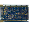
Contact us if you need more details on Double Sided Pcb Through Hole. We are ready to answer your questions on packaging, logistics, certification or any other aspects about Double Sided Pcb Board Prototype Kit、Standard Double Sided Pcb. If these products fail to match your need, please contact us and we would like to provide relevant information.
Product Categories : 0-18Layer FR4 Board > 6 Layer Laser Circuits